
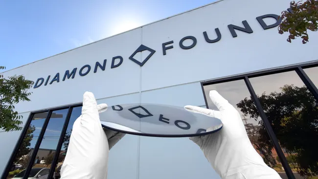
Diamond Foundry unveils the world’s first 200mm single-crystal diamond wafer, opening new possibilities for cooling increasingly powerful AI processors.
Diamonds have long been recognised for their exceptional physical properties, but their potential extends well beyond jewellery. A major development in synthetic diamond technology could see diamonds play an increasingly important role in the future of artificial intelligence, advanced computing and semiconductor manufacturing.
US-based Diamond Foundry has announced what it describes as the world’s first 200mm single-crystal diamond wafer, marking a significant milestone in the development of industrial applications for lab-grown diamonds.
The breakthrough could help address one of the biggest challenges facing the technology industry: managing the enormous amounts of heat generated by increasingly powerful computer chips.
Why diamonds could be the answer to AI cooling
Diamond is one of the most thermally conductive materials known to science. Its ability to transfer heat is exceptional, with high-quality single-crystal diamond capable of conducting heat at several times the rate of copper.
This makes it particularly attractive for semiconductor applications, where heat management has become increasingly important as processors become smaller, faster and more powerful.
Modern AI processors generate substantial heat, creating thermal hotspots that can affect performance, reliability and energy efficiency. Conventional cooling materials are increasingly being challenged by the demands of high-performance computing.
Single-crystal diamond offers a potentially important solution. It combines outstanding thermal conductivity with excellent electrical insulation, allowing heat to be moved away from sensitive electronic components without interfering with their electrical operation.
From laboratory development to wafer-scale manufacturing
What makes Diamond Foundry’s achievement particularly significant is the scale of the material.
Unlike conventional polycrystalline synthetic diamond, which consists of numerous smaller crystal grains, single-crystal diamond has a continuous crystal structure. This distinction is important because it allows the material to retain the exceptional thermal properties required for advanced semiconductor applications.
Producing large, high-quality single-crystal diamond wafers has been a considerable scientific and engineering challenge for decades.
The new 200mm wafer represents an important step towards making the material commercially viable for semiconductor manufacturers. The company has also indicated that producing 300mm diamond wafers could become achievable before 2030, potentially bringing diamond-based technology closer to the requirements of advanced semiconductor fabrication.
However, the achievement is still an important development rather than a finished commercial product. The demonstration wafer requires further processing and polishing before it can be incorporated into semiconductor manufacturing systems.
A technology industry increasingly turning to synthetic diamonds
Diamond Foundry is not alone in exploring the industrial potential of lab-grown diamonds.
Several major technology companies and research groups are investigating diamond-based materials to improve thermal management in next-generation electronics.
These include:
- Akash Systems: Developing gallium nitride technology integrated with synthetic diamond, targeting improved thermal performance in advanced electronic devices.
- De Beers Group: Exploring copper-plated diamond composite materials designed to improve cooling in AI computing, high-performance processors and radio-frequency applications.
- Frore Systems: Investigating diamond-enhanced cooling solutions for advanced graphics processors and high-performance computing systems.
The growing interest from these companies highlights how synthetic diamonds are moving beyond their traditional applications and becoming increasingly relevant to advanced manufacturing and technology.
The future of diamonds extends far beyond jewellery
For the diamond industry, developments such as this demonstrate the extraordinary versatility of diamond as an engineered material.
While natural diamonds remain highly valued for their rarity, geological origins and enduring appeal in jewellery, laboratory-grown diamonds offer manufacturers the ability to produce specialised materials with controlled characteristics for specific industrial applications.
From semiconductor cooling and quantum technology to optical systems, precision engineering and advanced electronics, the potential applications of synthetic diamonds continue to expand.
Diamond Foundry’s 200mm wafer is an important milestone in this evolution. Although widespread commercial adoption will require further development, it demonstrates that diamond technology may soon become part of the infrastructure powering the next generation of artificial intelligence.
The future of diamonds may not only be found in jewellery showcases, but also at the heart of the world’s most advanced technology.
Not All Lab-Grown Diamonds Are the Same
It is important to distinguish between laboratory-grown diamonds manufactured for the jewellery industry and the specialised synthetic diamonds being developed for advanced industrial applications.
Both are real diamonds, with the same fundamental chemical composition and crystal structure as natural diamonds: pure carbon arranged in a diamond crystal lattice. However, their intended applications, manufacturing requirements and specifications can be very different.
Gem-quality lab-grown diamonds are produced using technologies such as High Pressure High Temperature (HPHT) and Chemical Vapour Deposition (CVD). They are manufactured to achieve the colour, clarity, cut and overall appearance required for jewellery. Like natural diamonds, they can be graded according to established gemmological standards.
Industrial single-crystal diamonds, such as the 200mm wafer developed by Diamond Foundry, are engineered for specific technical applications. Their priority is not beauty, brilliance or jewellery grading, but crystal quality, thermal conductivity, consistency and the ability to manufacture large, uniform structures.
There is also an important distinction between single-crystal and polycrystalline diamond. Single-crystal diamond has one continuous crystal lattice, while polycrystalline diamond consists of numerous smaller diamond crystals joined together. This difference can significantly influence thermal and other physical properties.
The Diamond Foundry development is therefore not simply about producing a larger laboratory-grown gemstone. It represents a major engineering achievement in manufacturing large-scale, specialised diamond material for semiconductor technology.
At DCLA, we recognise that diamonds have applications extending well beyond jewellery. Understanding the differences between natural diamonds, gem-quality laboratory-grown diamonds and industrial synthetic diamond materials is increasingly important as diamond technology continues to evolve.
Comments are closed